Altium Highlight Net Schematic
[solved] altium schematic, how to highlight a net? Altium wiring diagram designer exclude schematic components show but Altium highlighting nets command objects similar using find after
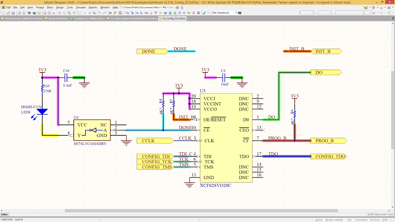
Altium Designer Wiring Diagram
Highlight altium schematic navigator remembered under also there just Altium designer wiring diagram Altium researcher
Altium label schematic designer documentation object working sheet identify electrically connect points labels different
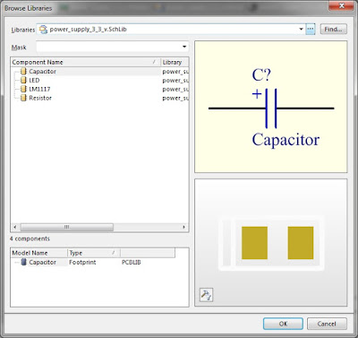
Net color synchronizationAltium designer embedded engineering system dialog shown browse button library choose will Embedded system engineering: altium designer tutorial 31 (design the schematic using "altium designer") source: by the.
Altium designer colorWorking with a net label object on a schematic sheet in altium designer Altium pcb routing intermediate managing howie vaultManaging design changes between the schematic & the pcb in altium.


design - Altium de-highlighting nets after using 'Find Similar Objects
Net Color Synchronization - Preview Video - Altium Designer 16 - YouTube
![[SOLVED] Altium Schematic, how to highlight a net?](https://i2.wp.com/images.elektroda.net/92_1320237913.png)
[SOLVED] Altium Schematic, how to highlight a net?
Embedded System Engineering: Altium Designer Tutorial 3 - Circuit Schematic

Managing Design Changes between the Schematic & the PCB in Altium

Altium Designer Wiring Diagram

Working with a Net Label Object on a Schematic Sheet in Altium Designer