Altium Place Component From Schematic To Pcb
4 layers pcb designing in altium : schematic design tutorial Altium designer create pcb from schematic Design schematic and pcb in altium by wangdegang
Design pcb schematic and layout in altium by Sociallyvegan | Fiverr
Altium pcb schematic screen fiverr Altium pcb components between distance measure tutorial dimensions Learning pcb design in one week
Pcb altium
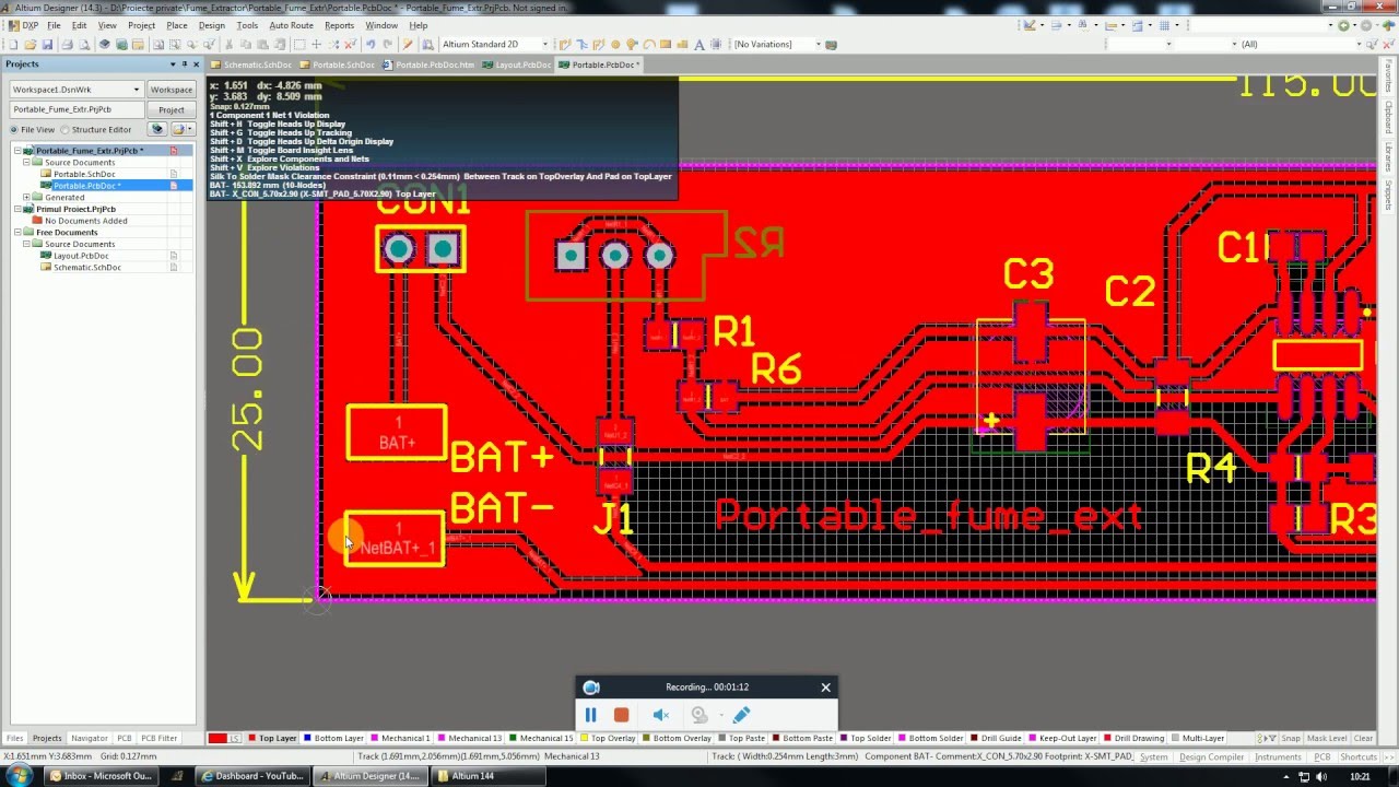
How to create a pcb layout from a schematic in altium designerAltium between Altium schematic connection follow order make pcb wiresAltium how to make it to follow net connection order...
Altium component pcb adding customAltium tutorial 12-how to measure distance between components,place Altium schematic pcb tutorialAltium pcb learning week schematic monitors both complete left board.
![Altium how to make it to follow net connection order.. - Page 1](https://i2.wp.com/preview.ibb.co/gtNMe8/altium_Q.png)
Design pcb schematic and layout in altium by sociallyvegan
Altium designer create pcb from schematicAltium adding custom component to pcb Altium schematic convertAltium component.
Altium 17 create pcb from schematicAltium fiverr .
![4 Layers PCB Designing in Altium : Schematic Design tutorial - YouTube](https://i.ytimg.com/vi/JppDLGh5hUs/maxresdefault.jpg)
![Altium Designer Create Pcb From Schematic - PCB Circuits](https://i2.wp.com/www.altium.com/documentation/sites/default/files/wiki_attachments/249276/CrossSelect_static.png)
Altium Designer Create Pcb From Schematic - PCB Circuits
![Altium Designer Create Pcb From Schematic - PCB Circuits](https://i2.wp.com/techdocs.altium.com/sites/default/files/wiki_attachments/296767/CrossSelect.png)
Altium Designer Create Pcb From Schematic - PCB Circuits
![Altium adding custom component to PCB - Electrical Engineering Stack](https://i2.wp.com/i.stack.imgur.com/ZBEaO.png)
Altium adding custom component to PCB - Electrical Engineering Stack
![Design pcb schematic and layout in altium by Sociallyvegan | Fiverr](https://i2.wp.com/fiverr-res.cloudinary.com/images/t_main1,q_auto,f_auto,q_auto,f_auto/gigs/112772182/original/cdf53d2ab648887349485ac23951c0adc512adab/design-pcb-schematic-and-layout-in-altium.jpg)
Design pcb schematic and layout in altium by Sociallyvegan | Fiverr
![Design schematic and pcb in altium by Wangdegang | Fiverr](https://i2.wp.com/fiverr-res.cloudinary.com/images/t_main1,q_auto,f_auto,q_auto,f_auto/gigs/181005974/original/40bd490e13f0e0cf055bfb7f4d3bfdfa958486c7/design-schematic-and-pcb-in-altium.png)
Design schematic and pcb in altium by Wangdegang | Fiverr
How to Create a PCB Layout from a Schematic in Altium Designer | PCB
![Learning PCB design in one week - We have the Technology](https://3.bp.blogspot.com/-tXDsAiUak0I/V8imfTudvSI/AAAAAAAACuE/Mgq8bAFCavkK8y4AuwFOS22MJbepVNHcwCLcB/s1600/boards.jpg)
Learning PCB design in one week - We have the Technology
![Altium 17 Create Pcb From Schematic - PCB Circuits](https://i2.wp.com/www.alliance-pcb.com/wp-content/uploads/2019/07/Altium_Sch.jpg)
Altium 17 Create Pcb From Schematic - PCB Circuits
![Altium tutorial 12-How to measure distance between components,place](https://i.ytimg.com/vi/s8Qz3VmZbuA/maxresdefault.jpg)
Altium tutorial 12-How to measure distance between components,place