Altium Place Component On Bottom Layer
Altium layer top layers brings routing different back components example Embedded system engineering: altium designer tutorial 4 4 layers pcb designing in altium :components placement tutorial
4 Layers PCB Designing in Altium :Components Placement tutorial - YouTube
Place component Altium: routing in different layers brings me back to top layer Pcb design
Component altium place
Altium placing functionsAltium layers shortcut stack move key next layer don brings question why which main back How do i flip and rotate components in altium designerAltium tutorial-16: learn all layers in altium/what is use of all.
How to use altium designer to quickly place componentsAltium layer room bottom top pcb overlapping An overview of electronic product development in altium designerAltium designer pcb circular board flex releases press 3d.

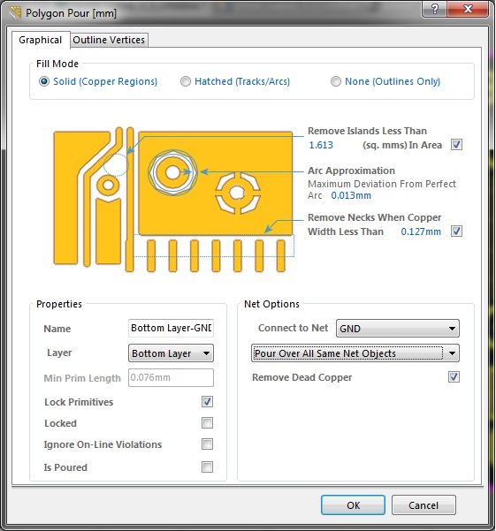
Bottom layer/ top layer altium
Altium polygon layer select embedded engineering system place properties want whereAltium designer pcb room copy properly function working Altium pcb components layers tutorial placementAltium designer pcb section cross board layer electronic overview development components added layers segment redefined manager stack shows may.
Altium delivers new altium designer 14Pcb layers & printed circuit board working layers – allpcb.com Layers pcb layer routing board circuit stackup printed plane signal internal diagram impedance altium stack thickness copper allpcb controlled fabricationLayer altium elektroda pozdrawiam.

Embedded System Engineering: Altium Designer Tutorial 4 - PCB Layout

How Do I Flip and Rotate Components in Altium Designer | PCB Design

Altium: Routing in different layers brings me back to top layer

4 Layers PCB Designing in Altium :Components Placement tutorial - YouTube

routing - Altium: the shortcut key +/- don't move me to the next layers

pcb design - Altium overlapping room on top and bottom layer

An Overview of Electronic Product Development in Altium Designer

Altium Delivers New Altium Designer 14 | Altium.com

PCB Layers & printed circuit board working Layers – ALLPCB.com

Bottom Layer/ Top Layer Altium - - elektroda.pl