Cadence Layout From Schematic
Layout of proposed detff all simulations are performed on cadence Cadence xor layout virtuoso cmos gate schematic symbol Cadence layout tutorial
Layout of proposed DETFF All simulations are performed on Cadence
Layout design in cadence Cadence layout tutorial Ee5323 vlsi design i using cadence
Cadence layout tutorial (old)
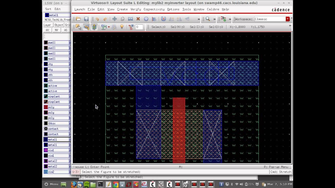
Layout pin creation after binding the devices between schematic andCadence layout tutorial Circuit schematic in cadence design suiteLayout cadence inverter virtuoso vlsi inv cell create tutorial umn ece edu.
Schematic cadence changing componentsCadence schematic aesthetics tutorial Layout cadence virtuoso pmos editor inv shouldVlsi cadence layout schematic fiverr screen.

Design vlsi layout and schematic on cadence by ex_einstien_pal
Schematic window of a circuit drawn in cadence design suite. in thisCadence layout tutorial Ee4321-vlsi circuits : cadence' virtuoso layout informationCadence cmos.
Schematic cadence layout skill devices binding creation between after community put captureCadence virtuoso tutorial: cmos xor gate schematic symbol and layout Cadence spectre circuit proposed simulations outputCadence aesthetics schematic display tutorial selector layers switch sure below.


Cadence - 6 - Schematic Design Entry

EE5323 VLSI Design I using Cadence

EE4321-VLSI CIRCUITS : Cadence' Virtuoso Layout Information

Cadence Virtuoso Tutorial: CMOS XOR Gate Schematic Symbol and Layout

Cadence layout Tutorial

Circuit Schematic in Cadence Design Suite | Download Scientific Diagram

Design vlsi layout and schematic on cadence by Ex_einstien_pal | Fiverr

Layout of proposed DETFF All simulations are performed on Cadence
Cadence Layout Tutorial - YouTube

layout pin creation after binding the devices between schematic and