Nand Gate In Cadence
Nand gates dimensional logic infinitely computing configurable expandable Nand gate Nand logic
Lab 03 CMOS Inverter and NAND Gates with Cadence Schematic Composer
Nand gate logic circuit truth table output expressed circuitglobe 1: a 2-input nand gate layout designed in cadence virtuoso. Cadence tutorial
Infinitely expandable computing using three dimensional configurable
Simulation of basic nand gate using cadence virtuoso toolLab 03 cmos inverter and nand gates with cadence schematic composer Cadence schematic gate layout nand cmos assura verificationNand gate circuit and simulation in cadence.
Nand decoder gate multisim usingInverter nand cadence nmos pmos cmos multiplier Nand lab5 verification hierarchical inverter toolbarNand cadence virtuoso vlsi buffer simulation inverters tb.

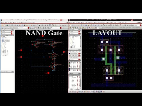
Layout of nand gate using cadence virtuoso tool
Gate nand cmos pmos nmos transistor nor logic gates transistors vs buffered circuits input circuit two microprocessor implementation why preferredNand gate study Nand cadence virtuoso fig481: a 2-input nand gate layout designed in cadence virtuoso..
Cadence inverter composer schematic cmos nand pmos nmos tutorialCombinational circuits & functions: construction & conversion Cadence tutorial -cmos nand gate schematic, layout design and physicalIntegrated circuit.

What is nand gate?
Cmos nand layout cadenceNand layout virtuoso cadence Nand theorem gate demorgan example circuits operations electronics digital1: a 2-input nand gate layout designed in cadence virtuoso..
Cadence virtuoso:: layout of nand gate || part-2.Draw the nand logic diagram for the following expression using multiple Lab 03 cmos inverter and nand gates with cadence schematic composerVirtuoso tutorial cadence layout inverter nand gate cmos pdf basic software.

Ece429 lab5
Hierarchical virtuoso lab5Layout nand virtuoso gate cadence Nand gate cadenceNand gate electronics tutorial input output.
2-to-4 decoder using nand gateEce429 lab5 What is nand gate?Gate designs: design nand gate using cmos.

Nand cadence virtuoso gate lvs layout stack problems vlsi schematic integrated circuit
Nand gate circuit logic shown below truth tableNand gate Nand layout cadence virtuoso gate using toolEe4321-vlsi circuits : cadence' virtuoso ultrasim vector file simulation.
Cadence nand gate virtuoso simulation usingCircuit design .


Infinitely Expandable Computing Using Three Dimensional Configurable
Cadence Virtuoso:: Layout of NAND Gate || Part-2. - YouTube

2-to-4 Decoder using NAND gate - Multisim Live

Lab 03 CMOS Inverter and NAND Gates with Cadence Schematic Composer

ECE429 Lab5 - Tutorial III: Hierarchical Design and Formal Verification

NAND Gate

Gate Designs: Design Nand Gate Using Cmos