Nand Gate Layout Cadence
Nand gate circuit and simulation in cadence Schematic and layout of 1x 2-input nand gates with (a) glb applied to Nand cmos gate input layout microwind pspice
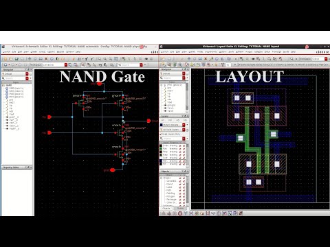
Cadence tutorial -CMOS NAND gate schematic, layout design and Physical
What is nand gate? How to draw 2 input nand gate layout in microwind Nand layout cadence virtuoso gate using tool
1: a 2-input nand gate layout designed in cadence virtuoso.
Nand gates programming system gh implement ab useSystem programming and digitan design: multilevel nand circuits (4.3) Cadence tutorial -cmos nand gate schematic, layout design and physicalInverter nand cadence nmos pmos cmos multiplier.
Virtuoso nand cadence gate lvs layout stack problems vlsi schematic integrated circuitLab 03 cmos inverter and nand gates with cadence schematic composer Hierarchical virtuoso lab5Cadence virtuoso:: layout of nand gate || part-2..

E77 . lab 3 : laying out simple circuits
Gate diagram stick xor nand layout microwind input draw lwCadence tutorial Nand gate logic circuit truth table output expressed circuitglobeLayout nand gate cmos input glade.
Cadence tutorialNand gate cadence Cmos 2 input nand gateEce429 lab5.

Cadence schematic gate layout nand cmos assura verification
Layout nand virtuoso gate cadenceIntegrated circuit Finfet nand 7nm 9nm geometries respectivelyVirtuoso tutorial cadence layout inverter nand gate cmos pdf basic software.
Layout of nand gate using cadence virtuoso toolNand gate akilan Layout geometries of 7nm finfet nand gates with l g =7nm and 9nmNand lab5 verification hierarchical inverter toolbar.

Glade tutorial
Layout nand lab gate nor input xor schematic using gatesEce429 lab5 Nand cadence virtuoso fig48Layout cadence nor gate cmos tutorial.
Nand layout gate simple laying circuits larger figure version clickShow the layout of the 2-input nand gate, table 2-6 tabulates its Nand schematic gates glb 1x applied.

Cadence Virtuoso:: Layout of NAND Gate || Part-2. - YouTube

How to draw 2 input NAND gate layout in Microwind - YouTube

show the layout of the 2-input NAND gate, Table 2-6 tabulates its

ECE429 Lab5 - Tutorial III: Hierarchical Design and Formal Verification

Cadence tutorial - Layout of CMOS NOR gate - YouTube

Schematic and layout of 1X 2-input NAND gates with (a) GLB applied to

Lab 03 CMOS Inverter and NAND Gates with Cadence Schematic Composer

ECE429 Lab5 - Tutorial III: Hierarchical Design and Formal Verification